Printed circuit board 'Multiuse PCB2'
Project overview
This small PCB, which I named Multiuse PCB2 is an improved version of multiuse tiny 1. I designed Multiuse tiny1 for my NES/SNES controllers to USB project. Since there is not a lot of space availabe inside an SNES controller, I designed the PCB to be as small as necessary. The PCB has improved since the beginning, thanks to the many other uses I found for this PCB.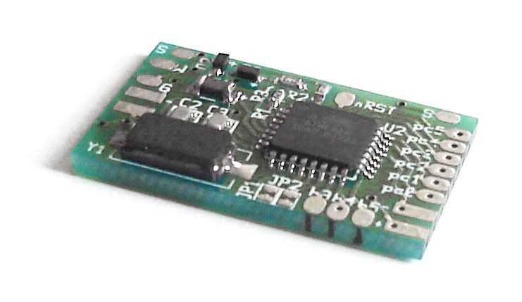
Top
- Small: width=27.5mm, height=17.7mm, thickness=3.4mm (without regulator) or 5.3mm (with regulator)
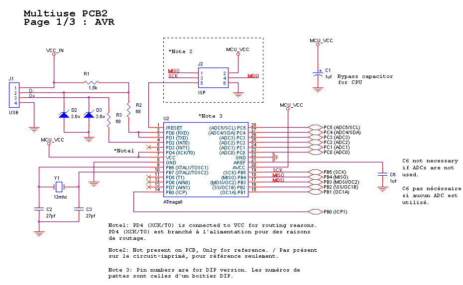
- Atmel AVR Atmega8 microcontroller on-board. Runs up to 16mhz.
- The following microcontroller signals are available via solder pads: PC5(ADC5/SCL), PC4(ADC4/SDA), PC3(ADC3), PC2(ADC2), PC1(ADC1), PC0(ADC0), PB5(SCK), PB4(MISO), PB3(MOSI), PB2(SS/OC1B), PB1(OC1A), PB0(ICP1), PD0(RXD), PD1(TXD), PD2(INT0). Please note that PD0(RXD) and PD1(TXD) are tied together.
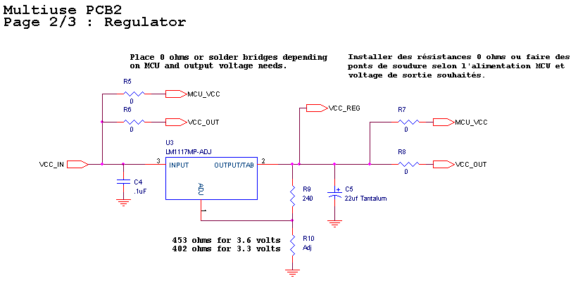
- Optional voltage regulator can supply a lower voltage to the MCU and/or external peripherals.
- This circuit is perfect for the Firmware-Only USB Driver from Objective development. All necessary components are there (Atmega8, 12mhz crystal with capacitors, 68 ohms resistors and zener diodes).
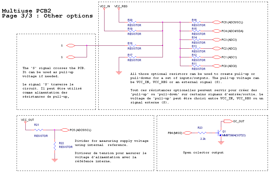
- Pull up or pull down (selectable) can be installed on many signals.
- Convenient pass through signal 'S' which crosses the board, but can optionally be connected to the pull-up/down array of resistors.

Bottom
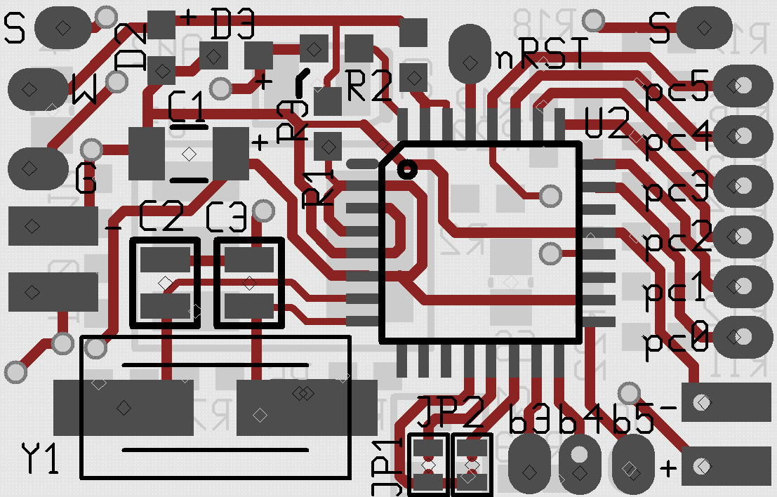
Schematic
The schematic is split on 3 different pages.Here is the the schematics in png format:
And in PDF format: multiuse_pcb2_schematic.pdf
Programming:
To program the microcontroller, the ISP wires must be soldered directly on the board. Look at the schematic for the locations.
If you are not familiar with the programming procedure for Atmel AVRs using ISP, consult my AVR programming page.
USB:
When USB is not used, it is not necessary to solder the zener diodes and R1. The 68 ohms resistors R2 and R3 may be replaced by 0 ohm resistors if you need to use those ports. (That's what I did for the SNES/NES Gamepad to Gamecube/Wii adapter project.
Regulator:
The PCB backside has a footprint for an lm1117 voltage regulator. 0 ohm resistors or solder bridges must be installed to select the power source for the microcontroller and the circuit output.
When no regulator is needed, installing U3, R9, R10, C5, R7 and R8 is not necessary. But don't forget to install R6, R7 and C1.
The voltage regulator has an adjustable output. Here is a convenient tool you can use to calculate the output voltage that would be obtained depending on the selected resistors.
PCB
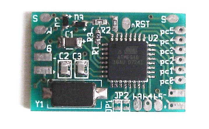
Top
The picture on the right shows the top side populated for USB communication (12mhz crystal, 68 ohm resistors, 1.5k resistor and two 3.6 volt zeners). Notice the two solder pad labelled 'S'. This is a pass-through signal that is useful for some adapters. This signal is also accesible on the back side via R18.

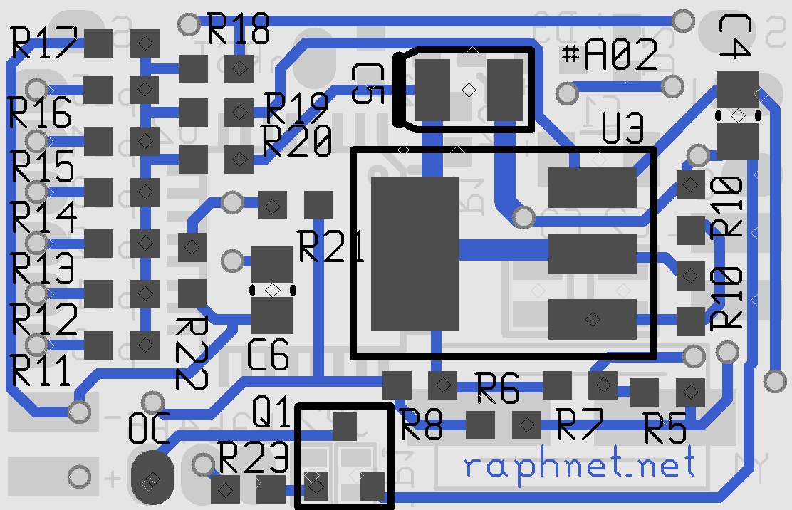
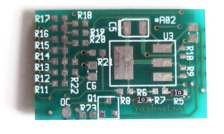
With regulator
The regulator used is an lm1117mp-adj. 0 ohm resistors must be installed in order to select the power source (Input voltage or regulator output voltage) of the microcontroller and the board power output.
For example, to supply 5 volts (from USB) to the microcontroller and 3.3 volts (regulator output) to a game controller, resistors R5 and R8 would have to be installed.
The picture on the right is an interesting example which demonstrates the circuit flexibility (for the gc/n64 to usb adapter). A regulator is installed with resistors for a 3.3 volts output. A pull-up is installed (R16, 2.2k) and is connected to 3.3 volts via R20 (0 ohms). The 'S' signal is connected to the input voltage (for this project, 5 volts from USB) by connecting R19 with R18 with a 0 ohm resistor.
Without regulator
When no voltage regulator is required, the only components that must be installed on the bottom side are two 0 ohm resistors. Install them according to the picture on the right. If you don't have 0 ohm resistors, use short pieces of wire or do a solder bridge.
Of course, even if there is no regulator, it's still possible to install pull-ups or pull-down resistors on many IOs.
Here are the gerber files which you may use to produce this PCB:
multiuse_pcb2.zip
Programming
Programming the circuit requires soldering the programmer wires at the correct spots or building a jig with correcly placed spring loaded contacts. Look at the schematic and note the MCU pin names where the ISP signals go:| Signal ISP | MCU Pin |
|---|---|
| SCK | PB5 |
| MISO | PB4 |
| MOSI | PB3 |
Then looking at the PCB, you should see labels B5, B4, B3 in the lower right. As you are probably already guessing, B5 is for PB5, B4 for PB4, etc. The reset signal is at the top, marked nRST. ISP gnd and vcc must also be connected, and remember that normally (at least, with the official mkII Atmel programmer) the programmer does not supply power.
Disclaimer
I cannot be held responsible for any damages that could occur to you or your equipment while following the procedures present on this page. Also, I GIVE ABSOLUTELY NO WARRANTY on the correctness and usability of the informations on this page. Please note, however, that the procedures above have worked in my case without any damages or problems.Now you cannot say that I did not warn you :)