Setting up the stack for SMS games on Megadrive
The problem

When an SMS game is run on a Megadrive console, there is no bios to run before the game. The CPU executes the game right from the start. This can be a problem for games which rely on intialization normally performed by the bios, in particular setting up the stack pointer.
A quick workaround to this is to first run an SMS game that does not have this problem, turn off the power, insert the non-starting game and reapply power. Now the game should start. This is because even following the power cycle, the stack pointer register bits haven not faded away yet and are still at the last value used!
While the above trick seems to work well, it is not ideal. One needs to repeat those steps every time, and one has to own at least one game that starts without problems.
Sega's solution for the Power base converter
Sega used to sold a product equivalent to my adapter under the names Power base converter, Mega Adaptor(メガアダプタ), Master System Converter or Adaptador Para os Jogos Master System according to the region of the world.[1].Sega's adapter did not have the game startup problem described in the previous paragraphs. An interesting discussion on smspower reveals that a simple programmable logic chip was used to have the CPU run a few instructions to setup the stack pointer prior to game execution:
	21 01 E1 : LD HL, $E101
	25 -- -- : DEC H
	F9 -- -- : LD SP,HL
	C7 -- -- : RST $00
The same thread also provides the chip's logic equations which shows how the address bits on the BUS are used to present the instruction bytes in consecutive order, and how a conflict between this chip and the cartridge is avoided by letting the chip enable signal run through this same chip. For complete technical details, please refer to the discussion.
Interesting fact: Since the logic chip did not have enough outputs to drive the BUS eight data bits, bit 0 is pulled high through a resistor. So the instructions shown above all have the less significant bit set to 1!
[1] Source: http://segaretro.org/Power_Base_Converter.
My hack using an AVR micro-controller
The MCU monitors the read signal (RD) and after each pulse, drives the next instruction value on the data bus, until all 6 bytes have been presented, after which all MCU pins are switched to input mode to let the game run without impediments.
The MCU does not monitor the CE signal since it is too slow to use it properly. The data lines are therefore continuously driven, where normally they would be driven only when CE and RD are low. This is not very clean, but since we are controlling the instructions the CPU is executing and know that none of them result in writes (until we let go of the bus), I don't think this is a problem.

I simply reproduced what Sega did for the D0 bit, even though I still had a free output on my MCU board (PORTB3). I don't remember why I did that (because I waited 3 months to write this article) but it might have been to simplify programming during development (one of the signals uses PORTB3). In any case, whatever the reason, a pull-up resistor must currently be installed on D0, but it would be easy to update the firmware to do away with this requirement.
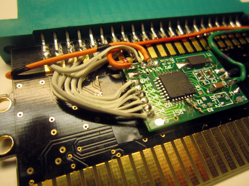
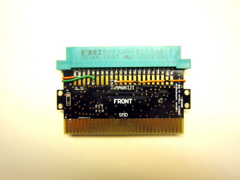
Here are a few pictures of the circuit installed on my cartridge adapter. If you built an adapter like mine or own a non-Sega adapter without the stack initialisation circuit, you could use this small circuit to fix the problem.
Contact me if you are interested and I will add preprogrammed circuits to the store.


Source code is available here:
stackchip.tar.gz
Here is an abridged version showing the essential parts:

During development
#define WAIT_RD()   do { } while (PIND & 0x04)
#define WAIT_RD_HIGH()  do { } while (!(PIND & 0x04))
#define OUTVAL(a,b) do { PORTC = a; PORTB = b | 0x10; } while(0)
#define RD_SYNC()   do { WAIT_RD(); WAIT_RD_HIGH(); } while(0)

...

/* LD HL, $E101 */
OUTVAL(0x10, 0x00);
RD_SYNC();
OUTVAL(0x00, 0x00);
RD_SYNC();
OUTVAL(0x70, 0x20);
RD_SYNC();

/* DEC H */
OUTVAL(0x12, 0x00);
RD_SYNC();

/* LD SP,HL */
OUTVAL(0x7C, 0x20);
RD_SYNC();

/* RST $00 */
OUTVAL(0x63, 0x20);
RD_SYNC();

// hands-off the bus
while (1) {
	DDRC = 0;
	DDRB = 0;
	set_sleep_mode(SLEEP_MODE_PWR_DOWN);
	sleep_enable();
	sleep_cpu();
}
Disclaimer
I cannot be held responsible for any damages that could occur to you or your equipment while following the procedures present on this page. Also, I GIVE ABSOLUTELY NO WARRANTY on the correctness and usability of the informations on this page. Please note, however, that the procedures above have worked in my case without any damages or problems.Now you cannot say that I did not warn you :)