RetroChallenge, September 2018
Summary
For the September 2018 edition of the RetroChallenge, I plan to look very carefully into a modem (and related items) for Super Famicom: The NDM24.With this modem connected to a controller port and with an unusual game controller, the NDK10, of which I documented the protocol in the past, the game cartridge JRA Pat apparently made it possible to place bets (real ones!) on horse races.
By trial and error, I modified an emulator and succeeded in tricking the game to think that a modem was present. But I only got past a simple test that did not involve data exchange. I reached a configuration screen, but could not get past: The game would hang with a "saving in progress" message...
Unable to quench my curiosity, I gave in and bought an NDM24 modem as well as a JRA PAT cartridge so I could probe the thing in action. And the items arrived just in time for the RetroChallenge!
So what I'm planning now is to:
- Find out how the modem communicates with the console through a controller port.
- Learn more about the modem. How fast (or slow) is it? Does it use standard AT commands?
- Attempt to make everything work in an emulator. (Communication with the modem and modem commands?)
- Pretend the connection succeeds to see what happens next.
- Attempt to understand how the nature of the exchanges between the game and the server.
Let's look at the "game"
So I connected the controller (port 1) and the modem (port 2) to my Super Nintendo system. When the modem is ON, the game does not display any error message and shows the title screen.学生・生徒・未成年者は勝馬投票券を購入することはできません
Purchase of betting tickets by students and minors is forbidden.
(Literal translation: Students and minors cannot buy betting tickets)
If like me you were wondering what JRA PAT meant, the title screen gives the answer.
JRA PAT = Japan Racing Association Personal Access Terminal
By pressing A, the game advances to another screen where one must enter his subscriber number and access code. Those are entered using the numerical buttons on the controller.
加入者番号とパスワードを入力して下さい。
Please enter your subscriber number and password.
Strangely enough, the game accepted whatever numbers I used and then displayed a box asking if I'd like to download up to date information. (no picture for this, sorry).
By answering NO (いいえ) to this message, I reached what appears to be the main menu:
Menu
投票: Bets
投票履歴: Bet history
照会: Requests (?)
情報取得: Acquire information
情報表示: Display informations
お知らせ: Announcements
投票要項取得: Acquire important betting information (?)
終了: Quit
The 情報取得 (Acquire information) menu choice opens another menu where one can build a list of information items to acquire:
Acquire information(Note: I am not very confident about those translations. I have not taken the time to become familiar with the world of horse race betting and the related vocabulary, and I don't know much about what variables are of interest for making a bet. In other words, I don't know what I'm talking about...)
開催案内: Guide/information about events (races?)
変更情報: Information about changes
オッズ: Odds
出馬表: Candidate table (?)
馬体重: Weight of the horses (?)
払戻情報: About refunds
競求項目確認: Bet confirmation
I selected " 開催案内: Guide/informations about events ", and it was added to the list of items to acquire. The game then asked if I wanted to add more items, or if I was ready to start the acquisition process. I answered YES (はい) to confirm that I was ready to establish a connection to the service center:
センタへ接続しますか?
Connect to the service center?
The modem "OH" indicator (Off hook) then turned on:

But of course, the call failed. No phone line is connected, but even then, it would not have worked. I am not in Japan, but more importantly, the service has probably ended long ago!
センタと接続できません。
再度通信
中止
通信設定の変更
コード390040019999
電話回線を確認して下さい。
Cannot connect to the service center.
Retry
Abort
Change connection parameters
Code 390040019999
Please check the phone line.
In order to let the connection succeed, I installed an internal US Robotics (USR) Sportster 28800 in an old computer and connected it directly to the Super Famicom modem (NDM24).
Luckily, the NDM24 does not seem to care if there is no dial tone. So injecting a tone with a signal generator was not necessary. The NDM24 simply dials despite the silence. However, as in such a setup there is no ring signal, I had to type ATA manually on the USR side as soon as the NDM24 had completed DTMF dialing.
Once the nostalgic chant of negotiating modems died, the game screen gave feedback about the successful connection with this screen with an animated running horse.
只今センタと通信中です。恐れ入りますが、そのままでしばらくお待ち下さい。
Presently communicating with the service center. Please keep waiting for a few moments.No problem, I'll just stare at the animation.
On the USR modem side, the words CONNECT 9600 indicated a successful connection at 9600 Baud. Every time I tried this (there are two attempts in the picture below) the game would send a few hundred bytes, the hang up after a few seconds. The game would then display a message saying that the server did not answer.
I captured what was received to a file for further analysis. Here is the data in hexdump format:
00000000  2b 2b 2b 61 74 68 0d 0d  0a 4f 4b 0d 0a 61 74 61  |+++ath...OK..ata|
00000010  0d 0d 0a 43 4f 4e 4e 45  43 54 20 39 36 30 30 0d  |...CONNECT 9600.|
00000020  0a 80 78 e0 f8 78 e0 80  78 fe 80 f8 f8 78 e0 78  |..x..x..x....x.x|
00000030  e0 78 e0 78 e0 78 e0 78  e0 78 e0 78 fe 80 f8 f8  |.x.x.x.x.x.x....|
00000040  f8 78 80 f8 78 e0 78 e0  78 78 1e 0f c0 78 1e f0  |.x..x.x.xx...x..|
00000050  80 78 e0 f8 78 e0 80 78  fe 80 f8 f8 78 e0 78 e0  |.x..x..x....x.x.|
00000060  78 e0 78 e0 78 e0 78 e0  78 e0 78 fe 80 f8 f8 f8  |x.x.x.x.x.x.....|
...
One thing that stroke me as odd when looking at the hexdump above was that all values were long sequences of 1s and 0s. It looked like a baud rate mismatch, as when the other end is sending slower than expected.
I was exchanging AT commands with the USR modem at 38400 BAUD. But the connection was being established at 9600. I thought the modem was supposed to convert the baud rate. Well it turns out that this is configurable. According to my modem manual, this is done using the
AT&B extended command:
Sure enough, verifying the current settings using
ATI4 confirmed that
the baud rate was indeed variable!So I issued theWonderful! I had not used this kind of modem for almost 15 years, doing it again was fun and I was even learning new things!
AT&B1 command to obtain a fixed baud rate.
Another solution would have been to change my terminal program (Telix 3.51) baud rate to 9600.This time, the data looked better, and I was able to spot some patterns.
	00000000  61 74 26 62 31 0d 0d 0a  4f 4b 0d 0a 61 74 61 0d  |at&b1...OK..ata.|
	00000010  0d 0a 43 4f 4e 4e 45 43  54 20 39 36 30 30 0d 0a  |..CONNECT 9600..|
	00000020  02 89 2f ae ba 94 94 94  94 94 94 94 9d bf 43 a4  |../...........C.|
	00000030  94 94 ba ba 3e 89 2f ae  ba 94 94 94 94 94 94 94  |....>./.........|
	00000040  9d bf 43 a4 94 94 ba ba  3e 0d 02 89 2f ae ba 94  |..C.....>.../...|
	00000050  94 94 94 94 94 94 9d bf  43 a4 94 94 ba ba 3e 89  |........C.....>.|
	00000060  2f ae ba 94 94 94 94 94  94 94 9d bf 43 a4 94 94  |/...........C...|
	00000070  ba ba 3e 0d 02 89 2f ae  ba 94 94 94 94 94 94 94  |..>.../.........|
	00000080  9d bf 43 a4 94 94 ba ba  3e 89 2f ae ba 94 94 94  |..C.....>./.....|
	00000090  94 94 94 94 9d bf 43 a4  94 94 ba ba 3e 0d db 2a  |......C.....>..*|
	000000a0  ef 77 77 77 77 77 77 9f  40 21 90 06 12 01 66 64  |.wwwwww.@!....fd|
	000000b0  11 88 44 20 21 c8 66 31  80 10 09 24 21 04 64 30  |..D !.f1...$!.d0|
	000000c0  91 c4 40 11 09 84 62 22  88 24 22 44 20 98 c0 20  |..@...b".$"D .. |
	000000d0  84 66 44 01 91 04 32 42  33 24 32 cc 24 13 44 22  |.fD...2B3$2.$.D"|
	000000e0  02 88 04 32 11 26 23 44  60 32 01 19 48 22 20 42  |...2.&#D`2..H" B|
	000000f0  21 0d 0a 4e 4f 20 43 41  52 52 49 45 52 0d 0a     |!..NO CARRIER..|
The above data did not come in all at once. It arrived in small chunks, I could tell simply by looking at the live terminal screen. In the hexdump above, I noted that those packets seem to start with 02 (STX) character and end with 0D (CR).
I observed that many characters had the most significant bit set, so I started wondering about parity. I had used a 8N1 setting when receiving the above..
So, should I try EVEN or ODD? I asked myself. I looked at several instances of characters to find out what was used:
- 89 : Binary 10001001. Number of 1s in the lower 7 bits: 2
- 94 : Binary 10010100. Number of 1s in the lower 7 bits: 2
- 9d : Binary 10011101. Number of 1s in the lower 7 bits: 4
- bf : Binary 10111111. Number of 1s in the lower 7 bits: 6
- 2f : Binary 00011111. Number of 1s in the lower 7 bits: 5
- 43 : binary 01000011. Number of 1s in the lower 7 bits: 3
Whenever the number of 1s found in the lower 7 bits was even, the most significant bit would be set, making
the total of bits set in the byte an odd value. So this system used odd parity! (unless it was an odd coincidence)With my terminal reconfigured for 7O1 communication, I got the following data:
	00000000  61 74 61 0d 0d 0a 43 4f  4e 4e 45 43 54 20 39 36  |ata...CONNECT 96|
	00000010  30 30 0d 0a 02 09 2f 2e  3a 14 14 14 14 14 14 14  |00..../.:.......|
	00000020  1d 57 2f 1d 14 14 20 3b  3e 09 2f 2e 3a 14 14 14  |.W/... ;>./.:...|
	00000030  14 14 14 14 1d 57 2f 1d  14 14 20 3b 3e 0d 02 09  |.....W/... ;>...|
	00000040  2f 2e 3a 14 14 14 14 14  14 14 1d 57 2f 1d 14 14  |/.:........W/...|
	00000050  20 3b 3e 09 2f 2e 3a 14  14 14 14 14 14 14 1d 57  | ;>./.:........W|
	00000060  2f 1d 14 14 20 3b 3e 0d  02 09 2f 2e 3a 14 14 14  |/... ;>.../.:...|
	00000070  14 14 14 14 1d 57 2f 1d  14 14 20 3b 3e 09 2f 2e  |.....W/... ;>./.|
	00000080  3a 14 14 14 14 14 14 14  1d 57 2f 1d 14 14 20 3b  |:........W/... ;|
	00000090  3e 0d 45 43 5c 77 77 77  77 77 77 77 06 12 01 66  |>.EC\wwwwwww...f|
	000000a0  64 03 09 40 33 01 06 11  09 66 12 10 20 19 40 20  |d..@3....f.. .@ |
	000000b0  22 10 42 09 44 62 20 30  19 48 04 66 11 01 40 62  |".B.Db 0.H.f..@b|
	000000c0  03 60 10 19 22 10 40 02  10 26 32 04 22 10 02 0d  |.`..".@..&2."...|
	000000d0  0a 4e 4f 20 43 41 52 52  49 45 52 0d 0a           |.NO CARRIER..|
Or if split according to what I think are packets:
- 02 09 2f 2e 3a 14 14 14 14 14 14 14 1d 57 2f 1d 14 14 20 3b 3e 09 2f 2e 3a 14 14 14 14 14 14 14 1d 57 2f 1d 14 14 20 3b 3e 0d
- 02 09 2f 2e 3a 14 14 14 14 14 14 14 1d 57 2f 1d 14 14 20 3b 3e 09 2f 2e 3a 14 14 14 14 14 14 14 1d 57 2f 1d 14 14 20 3b 3e 0d
- 02 09 2f 2e 3a 14 14 14 14 14 14 14 1d 57 2f 1d 14 14 20 3b 3e 09 2f 2e 3a 14 14 14 14 14 14 14 1d 57 2f 1d 14 14 20 3b 3e 0d
- 02
- 09 2f 2e 3a 14 14 14 14 14 14 14 1d 57 2f 1d 14 14 20 3b 3e
- 09 2f 2e 3a 14 14 14 14 14 14 14 1d 57 2f 1d 14 14 20 3b 3e
- 11111111:1111 :: 09 2f 2e 3a 14 14 14 14 14 14 14 3a 3a 3a 3a 14 14 3a 3a 3e
- 11111112:1111 :: 09 2f 2e 3a 14 14 14 14 14 14 14 3a 3a 3a 1d 14 14 3a 3a 3e
- 11111113:1111 :: 09 2f 2e 3a 14 14 14 14 14 14 14 3a 3a 3a 5e 14 14 3a 3a 3e
- 12412312:9876 :: 09 2f 2e 3a 14 14 14 14 14 14 14 1d 6d 2f 1d 14 14 20 3b 3e
- 12312312:9876 :: 09 2f 2e 3a 14 14 14 14 14 14 14 1d 57 2f 1d 14 14 20 3b 3e
- 01020304:0506 :: 09 2f 2e 3a 14 14 14 14 14 14 14 62 49 79 25 14 14 32 4c 3e
- 07080910:1415 :: 09 2f 2e 3a 14 14 14 14 14 14 14 4d 7d 65 33 14 14 6b 76 3e
- 16171819:2021 :: 09 2f 2e 3a 14 14 14 14 14 14 14 12 70 18 71 14 14 73 38 3e
- 22232425:2627 :: 09 2f 2e 3a 14 14 14 14 14 14 14 5c 2f 47 17 14 14 11 40 3e
Yes, what the game sends varies according to the username and password. What appears
to be the user id field is in underline and what appears to be the password is in bold.I tried a few approaches, but I could not find a simple way to decode the numbers (besides making a table obviously). But this is not important at this point. If I knew how to decode the values above, what would be the use of it? I was just curious.
Clearly, this system is designed to work off line and minimize the time the phone line is used.
This is a bit unfortunate, I admit I was hoping for something a bit more "dumb" where data received from the modem would go straight to the screen and where the controller buttons would simply send characters to the modem. (That would have opened the door to fun things, such as controlling a Linux box from a Super NES...)
Let's look inside the modem
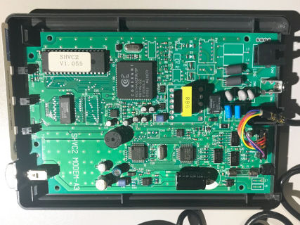
Here is a picture of the NDM24 internals:This modem is based on the RCV144ACFW/SP chip (Rockwell / Conexant) which can communicate up to 14400 baud and offers a serial interface to the controlling terminal/PC.
Here is my interpretation of the design:

In blue: Power supply
Nothing special.In yellow: The RCV144ACFW < > Super Famicom interface
The RCV144ACFW (model R6746) is designed for asynchronous serial communications, i.e. RS-232. If this was a "standard" modem for use on a PC, the serial IOs would simply go through a level converter (0-5 volt on the RCV144 side, +12 to -12v on the PC side). But the NDM24 connects to a Super Famicom controller port. Of course, this is not supported by the RCV144! As a result, something has to translate between the two.Translation between the Super Famicom and the RCV144 is, as far as I can tell, taken care of by two ICs. (IC10: 78081GA57 9937PP002, IC9: D65611 026 9948LY009). I don't have any info about what those are exactly.
In the picture above, an unpopulated connector footprint is present. There is only one thing to do when discovering somthing like this: Probe the thing!
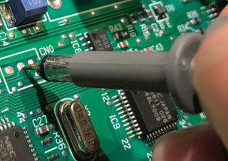
With a scope, I observed data exchanges timed at 19200 baud. This connector was probably used for monitoring the data exchanged between the RCV144ACFW and the Super Famicom. Perfect for development!
I decoded one of the traces I captured, and it really looks like exchanges with a modem. Below: [CR][LF]OK[CR][LF]

In purple: The modem
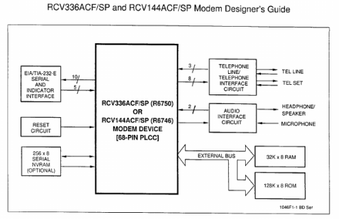
The main IC (RCV144ACFW) is accompanied by ROM and RAM on the left, and on the right, by the group of components necessary for interfacing with the phone line: Transformer, off-hook relay, surge protectors and filters, etc).As one would expect, overall it is very similar to this diagram found in the RCV144 design guide:
In red: Missing components
There are several unpopulated footprints in the phone line interface. Based on the following diagram, also from the RCV144 design guide, I would say that the missing features are:- Ring detection circuit. (Opto-isolator PC2 is not installed.)
- No relay to disconnect the handset. (This modem does not have the second connector where one would normally connect a normal phone)
A start at emulation
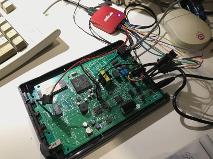
This week-end I was planning to use a scope to inspect the signals between the console and the modem, and then confirm my observations by getting the game to work in an emulator.I chose to use the bsnes-plus emulator as work tool due to its debugging features which I think will be useful.
I already had done quick and dirty modifications to higan to get past a simple controller and modem presence test. This week I did the same to bsnes-plus, but cleanly this time: The NTT Data Keypad and Data Modem options appear where they should in the menus, and the additional controller buttons are actually usable. The modem part however merely returns the correct id at clock cycles 12 to 15.
My modified bsnes-plus version, with controller and (incomplete as of now) modem support is on github: https://github.com/raphnet/bsnes-plus/tree/ntt_data_keypad_and_modem
However, despite support for the NTT Data Keypad and the modem in the emulator, some JRA PAT versions display an error screen at startup:
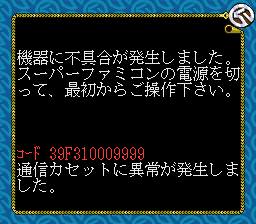
機器に不具合が発生しました。スーパーファミコンの電源を切って、最初から機動下さい。
コードー39F310009999
通信カセットに異常が発生しました。
An equipment problem has occured. Please turn off your super famicom and try again.
Code 39F310009999
An error has occured in the cartridge. (lit.: Communication cartridge)
An error has occured in the "Communication cartridge"? I assume this just means the cartridge. (and not an X-band style modem!). Here is what my cartridge contains:
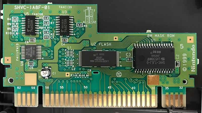
OK, so the ICs are:
- U4: Nintendo's CIC chip
- U5: Standard logic IC 74AC08 (Quad 2-input AND gate)
- U3: Standard logic IC 74AC139 (Décodeur/démultiplexeur 2 à 4)
- U2: A SHARP FLASH memory IC: LH28F020SUT-N80 (2MBIT / 256x8)
- U1: The game ROM. (Apparently 8MBIT / 1024x8)
The emulator probably does not emulate the flash chip, and I think this is why the game displays an error. Unlike ROMs or EPROMs, flash memory chips support commands to read its ID, unlock write mode and so on. It is reasonable to expect software to at least check the ID at startup.
Implementing support for this SHARP Flash chip in the emulator appears to be the necessary next step.
New goals
OK, I just discovered that the nocash SNES documentation covers almost everything I wanted to find out:- Information about the flash chips used by different versions of the game: http://problemkaputt.de/fullsnes.htm#snescartflashbackup
- How the modem communicates: SNES Add-On SFC Modem - Data I/O
- About the different modem versions: SNES Add-On SFC Modem - Misc
- Even the controller was documented: SNES Controllers NTT Data Pad (joypad with numeric keypad)
Oh no, all I was looking forward to discovering by my self is already documented! :(
I was naive enough to think I would be treading unknown ground, probing an unusual peripheral
with my oscilloscope, but everything is already known. And
yes, this is happening despite the research I did before starting this project.Only seven days in RC2018/09, and most items on my list are striken down:
Find out how the modem communicates with the console through a controller port.Learn more about the modem. How fast (or slow) is it? Does it use standard AT commands?Pretend the connection succeeds to see what happens next.
- Attempt to make everything work in an emulator. (Communication with the modem and modem commands?)
- Attempt to understand how the nature of the exchanges between the game and the server.
Thinking about the fact that very soon I will have a developer-friendly emulator supporting the controller and the modem, I got new ideas:
- Begin doing SNES programming
- Write code to read the NTT Data Keypad
- Write code to communicate with the modem
- Create a simple SNES terminal
My first SNES program
OK, so before adding support for a FLASH chip in bsnes-plus, I decided to teach myself a bit of SNES programming in assembly. But the SNES has a 65816 CPU for which I had never written any code.My assembly programming background:
I did a very tiny bit of 6502 assembly 13 years ago to fix the color palette of Super Mario Bros VS. when running on a standard NES, but then I forgot everything. So despite the 65816 being an extension of the 6502, I did not have a headstart.A few years later, I wrote a lot of Atmega AVR assembly code and some ARM assembly (mostly to speed up graphics using the iWMMX features of the Xscale).
And for the last 2 years, I have been writing Intel 8088 assembly for programming DOS games, such as RATillery.
My first steps with the 65816:
When I began using the 8088, it felt like a very limited CPU. I was used to RISC CPUs with a lot of registers, so I had to change my way of thinking and developed new strategies to accomplish what I wanted. I got the same kind of feeling, but this time with the 65816. It has even fewer registers than the 8088, they are specialized and even change size! I am not accustomed at all to programming for this type of architecture.As one would expect, I fell into a few traps:
- Failing to ascertain the state of the carry flag before doing an addition. This took me a while to figure out, because it was in a routine I did not write, which broke when the carry flag was set.
- Changing the size of the accumulator in a function or macro but not restoring it, breaking the assumptions of the caller.
- Failing to set the desired size of the accumulator or index registers in a macro or function, then having it fail after changing code before the call.
- Transferring a value from a 8-bit register to a 16-bit register (with TAY for instance) copies the "phantom" value from the high byte to the destination instead of zeroing the high byte of the destination. (Reading the manual helps!)
Results!
So after several hours of reading documentation, playing around with examples, reviewing tutorials and getting increasingly familiar with the debugging features built into bsnes-plus, I finally managed to create a simple ROM, a controller test supporting the NTT Data Keypad!Buttons that are pressed (or bits that read as logic low on the wire) are highlighted using the green squares. This includes the 4 ID bits. In the screenshot below, there was an NTT Data Keypad in port 1 and a Data modem in port 2. The keypad buttons 3, 6 and 8 were being held down.

It's basic, but at least there is some color. And just for fun, I made a scrolling background. It's common in SNES games, and I can see why given how easy and cheap this "effect" is on SNES.
My code uses the "old style" registers $4016 and $4017 to generate a latch pulse and then clock in 32 bits from the controller. I did not add delays between clock pulses and I have no idea if this is OK on real hardware. Nor do I know if this ROM works at all on real hardware. This will have to wait until I receive a flash cartridge I recently ordered. Update! It works fine on real hardware.
| Version 1.0 September 9, 2018 (Sunday) |
|---|
| First release. Has not been tested on real hardware |
| File(s): test32.zip (2.1 KB) |
Flash emulation
My JRA PAT (TJEJ) cartridge contains a LH28F020SUT-N80 flash chip. The excellent Nocash SNES documentation explains that there different JRA PAT versions and specifies which type of flash chip each one supports. The oldest version (TJAJ?) apparently supports only an AMD chip while later version support 3 type of chips (made by Amd, Atmel or Sharp).I decided to emulate the AMD chip since it is supported by all versions.
The Nocash documentation also provides information about how the flash chip is mapped in the SNES CPU's address space:
C0h-C3h:0000h-7FFFh ;128Kbyte FLASH (broken into 4 chunks of 32Kbytes)Reading from a flash chip like this one is like reading from RAM or ROM. But writing is a different story. Simply attempting to write to those addresses as if it were RAM normally won't have an effect. However, when some magic values are written at the right addresses, the flash enters command mode. It then becomes possible to read its manufacturer and device ID, erase parts of the flash or to write data to it.
For instance, to read the chip ID, and therefore detect the brand and model, here is what must be done:
- Write $AA to adresse $5555
- Write $55 to adresse $2AAA
- Write $F0 to adresse $5555
- Read the manufacturer ID from address $0000
- Read the product ID from adresse $0001
- .. and later exit this mode using another special sequence ..
I used the OBC1 code as an example how to implement the Memory interface, where one can catch reads and writes taking place in the particular address range the device is mapped to. This is what I needed to add support for the special sequence above. In order to preserve the flash contents across emulator restarts, I reproduced what was already there for battery backed RAM (The typical way games are saved on the SNES). With my modifications, a 128KB file ending with a .FLH extention is created.
But the emulator needs to be told that an AMD flash chip is present. This can be taken care of by a manifest. This manifest is a .xml file named after the rom file. For instance, if you are using JRA_PAT_TDEJ.sfc, you'll want to create JRA_PAT_TDEJ.xml. Here is what mine looks like:
<?xml version='1.0' encoding='UTF-8'?>
<cartridge region='NTSC'>
	<rom>
		<map mode='linear' address='00-9f:8000-ffff'/>
	</rom>
	<amdflash>
		<map mode='linear' address='C0-C3:0000-7FFF'/>
	</amdflash>
</cartridge>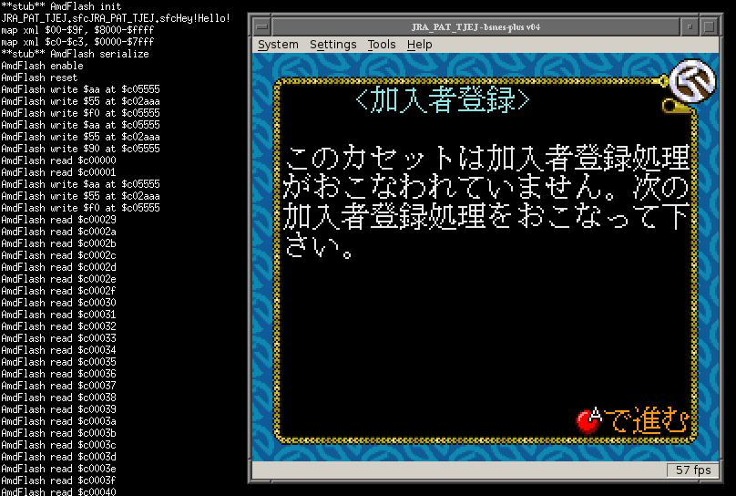
<加入者登録>
このカセットは加入者登録処理がおこなわれていません。次の加入者登録処理をおこなって下さい。
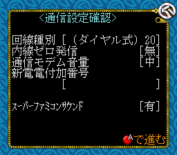
[Subscriber registration]First, communication parameters must be set.
The subscriber registration process has not been completed with this cartridge. Please complete the following registration process.

1. 回線種別 「20」 10 PBTranslation attempt:
2. 内線ゼロ発信 「無」有
3. 通信モデム音量 無 小 「中」大
4. 新電電付加番号
5. スーパーファミコンサウンド 無 「有」
6. 入力終了
1. Line classification (20 / 10 / PB). (*)
2. Operator call? (calling using 0 first? Not sure what this is)
3. Modem speaker volume (Mute / Low / Average / High)
4. Call prefix? Additional digits prepended to the number? (Not sure what this is yet)
5. Super Famicom sound (Off / On)
6. Apply (saves the parameters)
(*) I think 10 and 20 refer to the pulse rate when dialing (i.e. 10 pulses per second vs. 20 pulses per second). And I believe that PB stands for « Push Button » and refers to DTMF dialing.
When I attempted to save the configuration parameters, the game attempted writingn to the flash, and failed as I had not yet implemented write support. Here is the error screen:
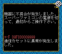
機器に不具合が発生しました。スーパーファミコンの電源を切って、最初から機動下さい。Here is a trace of what the game had just done.
コードー39F330009999
通信カセットに異常が発生しました。
An equipment problem has occured. Please turn off your super famicom and try again.
Code 39F330009999
An error has occured in the cartridge. (lit.: Communication cartridge)
....
AmdFlash write $aa at $c05555
AmdFlash write $55 at $c02aaa
AmdFlash write $90 at $c05555 ; Enter ID mode
AmdFlash read $c00000 ; Manufacturer
AmdFlash read $c00001 ; Device type
AmdFlash write $aa at $c05555
AmdFlash write $55 at $c02aaa
AmdFlash write $f0 at $c05555 ; End
...
AmdFlash write $aa at $c05555
AmdFlash write $55 at $c02aaa
AmdFlash write $80 at $c05555 ; Prepare for erase

AmdFlash write $aa at $c05555
AmdFlash write $55 at $c02aaa
AmdFlash write $30 at $c00000 ; Erase one 16k sector

AmdFlash read $c00000 ; Polls the progress of the erase. (Bit 7 is high, meaning it's done)

AmdFlash write $aa at $c05555
AmdFlash write $55 at $c02aaa
AmdFlash write $f0 at $c05555 ; End

AmdFlash write $aa at $c05555
AmdFlash write $55 at $c02aaa
AmdFlash write $a0 at $c05555 ; Write byte mode

AmdFlash write $01 at $c00000 ; Write value $01 to address $0000

AmdFlash read $c00000 ; Read the status of the write (returned $FF due to incomplete implementation)
AmdFlash read $c00000 ; Read the status of the write (returned $FF due to incomplete implementation)

; At this point the error message appeared.
This confirmed that I was on the right track. After that I spent a few minutes adding write support.
You may be wondering what the flash emulation code looks like. First, here is how read acceses are managed. All reads simply return the flash content, except if it is in ID, erase or write mode.
On real hardware, erase and write operations need some time to complete, and the code is expected to poll a status bit before starting another operation or reading. But my current goal is to reach the point where the game actually uses the modem to communicate, not to implement very accurate flash emulation. So at the moment all operations complete immediately without delays.
uint8 AmdFlash::read(unsigned addr)
{
  addr &= 0x1FFFF;
  switch (flash_state)
  {
      default:
        flash_state = StateNormal;
      case StateNormal:
        return memory::cartflash.read(addr);

      case StateId:
        if (addr == 0x0000) {
            return 0x01; // manufacturer
        }
        if (addr == 0x0001) {
            return 0x20;
        }
        return 0xff; // not sure

      case StateEraseAll:
        flash_state = StateNormal;
        return 0x80; // instantaneous!

      case StateEraseSector:
        flash_state = StateNormal;
        return 0x80; // instantaneous!

      case StateWriteByte:
        // Again, no attempt to provide realistic timing.
        flash_state = StateNormal;
        return (dta & 0x80);
  }
}
void AmdFlash::write(unsigned addr, uint8 data)
{
  int i;
  addr &= 0x1FFFF;

  if (flash_state == StateWriteByte) {
    dta = data;
    memory::cartflash.write(addr, data);
    flash_state = StateNormal;
    return;
  }

  if (step == 1) {
    if ((addr == 0x2AAA) && (data == 0x55)) {
      step++;
      return;
    }
    else
      step = 0;
  }
  if ((step == 0) && (addr == 0x5555) && (data == 0xAA)) {
    step++;
    return;
  };

  if (step < 2)
      return;

  step = 0;

  switch (data)
  {
    default:
      printf("unknown flash command 0x%02x\n", data);
      flash_state = StateNormal;
      break;

    case 0x90: // enter ID mode
      if (addr != 0x5555) {
        break;
      }
      flash_state = StateId;
      break;

    case 0xF0: // end / return to normal mode
      flash_state = StateNormal;
      break;

    case 0x80: // prepare erase (unlock?)
      if (addr != 0x5555) { step = 0; break; }
      flash_state = StatePrepareErase;
      break;

     case 0x10: // erase all
       if (addr != 0x5555) { step = 0; break; }
       for (i=0; i<0x20000; i++)
         memory::cartflash.write(addr+i, 0xFF);
       flash_state = StateEraseAll;
       break;

     case 0x30: // erase 16kb sector
       for (i=0; i<0x4000; i++)
         memory::cartflash.write((addr&0x1C000)+i, 0xFF);
       flash_state = StateEraseSector;
       break;

     case 0xA0: // write byte
       if (addr != 0x5555) { step = 0; break; }
       flash_state = StateWriteByte;
       break;
  }
}
Pressing A advances to the next step, where subscriber information must be entered.

加入者番号 [ ]
パスワード [ ]
生年月日 (西暦)[ …年 …月 …日]
入力終了(センタ接続)
Subscriber number [ ]
Access code [ ]
Birth date (AD) [___Year ___Month ___Day]
Confirm (and connect to the service center)
After hitting confirm, the software asks permission before connecting to the service center using the modem:

And finally! The screen with the animated horse where the modem starts being used is reached.
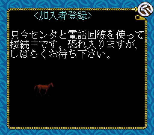
只今センタと電話回線を使って接続中です。恐れ入りますが、そのままでしばらくお待ち下さい。
Currently using the phone line to establish a connection to the service center. Please keep waiting for a few moments.
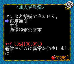
No surprise, the call fails since the modem is not emulated correctly. The error messages indicates an error with the modem (通信モデム) and offers 3 choices: To retry, To abort or to edit communication settings.
That's all for now. The modified bsnes-plus emulator I used is available in this github branch: https://github.com/raphnet/bsnes-plus/tree/ntt_data_keypad_and_modem
Modem monologue
How the modem communicates with the console is well documented in Nocash's SNES documenation:http://problemkaputt.de/fullsnes.htm#snesaddonsfcmodemdataio
So I added code to send/receive bytes according to the documentation, and also created a class meant to act (eventually) as a modem supporting AT commands. I got transmission (SFC to Modem) working first and simply sent the bytes to the terminal window.
This confirmed what I had heard, that standard AT commands were used. The game sends the following command in a loop:
ATE1Q0V1 : Enable echo (E1), Display result codes (Q0) and use english result codes (V1).Unfortunately, no matter what I do, the game does not accept what I send in reply to this command...
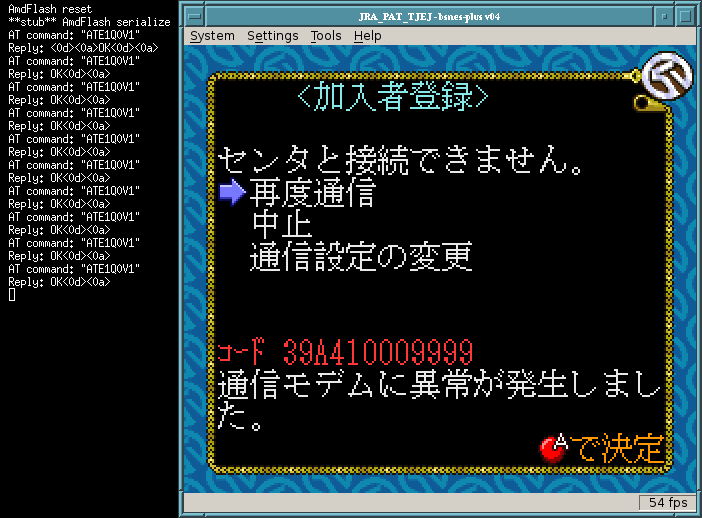
(Note: My implementation does supports echo. But the echoed characters are not visible above.)
After 10 unsuccessful attempts, the game gives up and displays an error message.
Why is it not working? There are many possible reasons.
- Error in my implementation (likely).
- I may have misunderstood the documentation (likely).
- While seemingly standard AT commands are sent to it, maybe the modem answers are not standard.
- There could be an error or omission in the documentation.
What would be most helpful now would be to have at an example of successful communication between the console and the modem. So it would appear that despite having found excellent documentation, I will still need to probe the signals on the modem PCB :)
My current version, which displays what the console sends but still fails to supply an acceptable answer for the game is here, just in case...
https://github.com/raphnet/bsnes-plus/tree/ntt_data_keypad_and_modem
Functional modem emulation
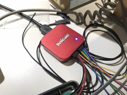
To understand what was wrong with my modem emulation code (the game was not accepting the answers from the fake modem) I gave attention to the original hardware.I obtained a small Saleae logic analyzer and installed probes on all signals between the Super Famicom and the modem, as well as on the modem debug port.
With such luxury, I easily confirmed that the debug port was as I expected. Right in between the console interface and the modem chip, one pin per direction (i.e. the TX and RX signals). I also learned that modems (or some/this modem) do not echo the \n character. This was a first thing to correct in my emulation code.

Next I looked at the first AT command transmitted by the game (ATE1Q0V1\r\n):

I noted that the RS232 transmission to the modem (line 01) starts while characters are still coming in from the console. So the circuitry between the RCV144 modem chip and the console has a bit of memory to do buffering. Here again, the modem echos all characters except \n.
Shortly after, the 9 echo characters are transmitted back to the SFC, pretty much as documented in the Nocash Full SNES doc:
- The first 8 bits on D0 (4017h.Bit0) contain one byte (when flagged as valid) from the modem.
- The 9th bit on D0 is a validity/presence flag for the above.

However when looking closely, I noticed that the second D1 bit (4017h.Bit1) was not working as I had understood from the documentation:

Some observations:
- The first transfer is 16 cycles long, the other only 9 cycles.
- The first transfer does not carry a valid byte from the modem (The 9th bit is 1)
- The second transfer (and the subsequent) do contain a byte from the modem
- The second bit on D1 (4017h.Bit1) is high only after the last byte is transmitted
- It is meant to notify the Super Famicom that the next transfer will contain a byte from the modem.
- The modem does not send bytes before first letting the console know about its intent to do so. (therefore, no data in the first transfer)
ATE1Q0V1
OK
ATE1Q0V1
OK
AT&F&W0&W1
OK
ATZ
OK
ATS7=60
OK
ATS8=3
OK
ATT
OK
ATL2
OK
AT%B9600
OK
AT\N0%C0
OK
ATS9=6
OK
ATS10=14
OK
ATS11=95
OK
ATS91=15
OK
ATX4
OK
ATD5555555
CONNECT 9600
When my code sees the AT%B9600 command (which purpose is, I think, to request a 9600 BAUD connection) it remembers it so it can repeat it after receiving the ATD command (so the game thinks it got exactly what it asked for). I'm not sure what settings would cause other speeds to be used, but the ROM do contain the strings AT%B2400 and AT%B1200)
Anyway, when the game receives "CONNECT 9600", the music changes and the horse starts galloping!
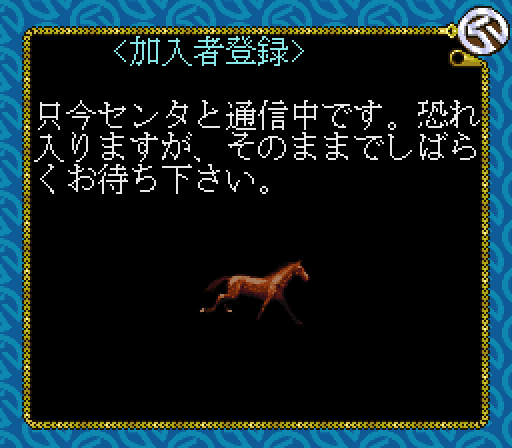
只今センタと通信中です。恐れ入りますが、そのままでしばらくお待ち下さい。
Presently communicating with the service center. Please keep waiting for a few moments.
A few seconds later, the game displayed a communication error message. No surprise there as there is still no server. The data the game sent was just going to a terminal window.
The following screenshot shows the data the game sent before aborting. And it matches what I got during the first week when I connected two modems together!
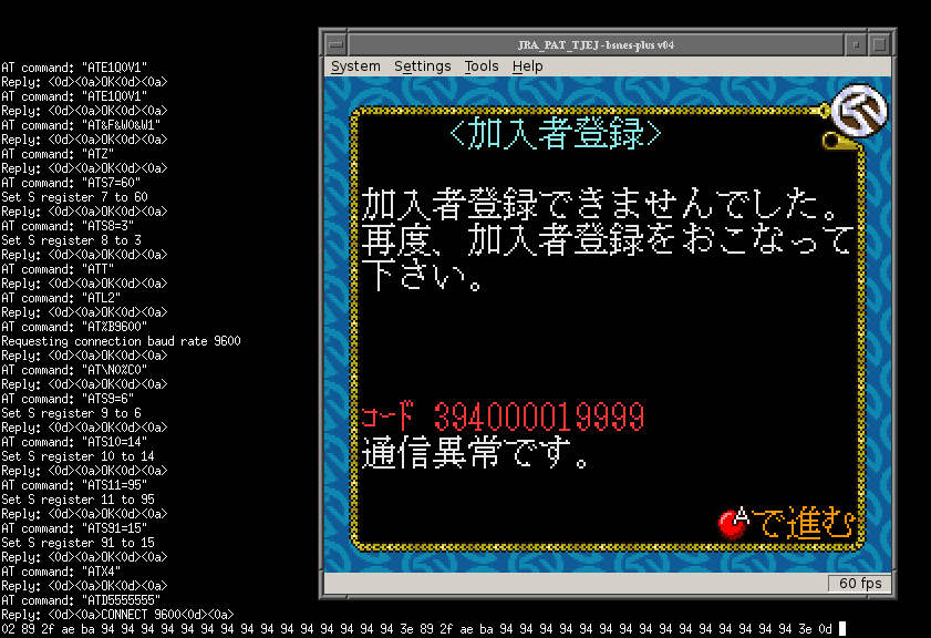
After displaying the communication error message, there is a menu with a retry option. But retries were not working since the modem was still "connected" (i.e. not in command mode) and no longer answered AT commands. This does not happen with the real modem. The game was making it hang up. But how exactly?
The Super Famicom sends data to the modem through register 4201h bit 7 which controls one of the controller connector pins. The first bit, when 0, indicates the following 8 bits are a valid byte from the console.
When there is not a valid byte, the bits are normally all 1s. However I observed that at the time the game wants to hang up, 0x43 (the ASCII for letter C) is sent instead:

I updated my emulation code again, and successive connection attempts became possible. But then I noticed that the game was aborting way earlier than it was on real hardware. During my tests using two modems, I had seen the game send several packets before aborting. However, when running in the emulator, the game would hang up after sending only one packet.
I wondered what it was the game did not "like" which made it trigger the premature hang up. And I also thought about, when the call is severed for external reasons (such as the classic "someone in the house picked up the phone") how do the game know?
I have some experience using serial modems, so I instantly thought about the DCD (Data Carrier Detect) signal which indicates an ongoing communication session with another modem, and I surmised that there had to be a bit somewhere in the exchanges with the Super Famicom corresponding to the carrier detect signal. This function not being emulated correctly yet, it could be that after sending a first packet, the game wrongly concluding that the connection had been cut!
To find out, I thought I'd compare the exchanges before the CONNECT 9600 message with those occurring after. I first located the message on the debug port:

Shortly after, those 16 bytes are relayed to the Super Famicom through the controller port:

Oh? There seem to be more pulses on the D1 line than previously! Let's see more closely:

Found it! The state of the D1 line on the seventh clock cycle is 0 when a carrier is present. (annotated with red dots)
The of course, I quickly added support for this to the emulator, and it worked! The game was now sending several packets before giving up.
TCP connection
The emulator uses a TCP socket instead of a phone line. When it receives the ATD command, instead of dialing (which it can't do), the emulator tries to connect to 127.0.0.1:5555. (Later I could use the phone number as an IP, for instance: 1270000000015555). If it succeeds, from this point the bytes sent by the game are forwarded through the socket.This means it would be possible to develop a server for the game. I will try to make sense of the exchanges, but I'm not sure how far I'll get. (I really have no idea what to answer). In any case, it is now very easy to capture what the game sends using netcat. For instance, I can do:
$ nc -l -p 5555 | hexdump -C
00000000  02 89 2f ae ba 94 94 94  94 94 94 94 94 94 94 94  |../.............|
00000010  94 94 94 94 3e 89 2f ae  ba 94 94 94 94 94 94 94  |....>./.........|
00000020  94 94 94 94 94 94 94 94  3e 0d 02 89 2f ae ba 94  |........>.../...|
00000030  94 94 94 94 94 94 94 94  94 94 94 94 94 94 3e 89  |..............>.|
00000040  2f ae ba 94 94 94 94 94  94 94 94 94 94 94 94 94  |/...............|
00000050  94 94 3e 0d 02 89 2f ae  ba 94 94 94 94 94 94 94  |..>.../.........|
00000060  94 94 94 94 94 94 94 94  3e 89 2f ae ba 94 94 94  |........>./.....|
00000070  94 94 94 94 94 94 94 94  94 94 94 94 3e 0d 02 89  |............>...|
00000080  2f ae ba 94 94 94 94 94  94 94 94 94 94 94 94 94  |/...............|
00000090  94 94 3e 89 2f ae ba 94  94 94 94 94 94 94 94 94  |..>./...........|
000000a0  94 94 94 94 94 94 3e 0d  02 89 2f ae ba 94 94 94  |......>.../.....|
000000b0  94 94 94 94 94 94 94 94  94 94 94 94 3e 89 2f ae  |............>./.|
000000c0  ba 94 94 94 94 94 94 94  94 94 94 94 94 94 94 94  |................|
000000d0  3e 0d                                             |>.|
https://github.com/raphnet/bsnes-plus/tree/ntt_data_keypad_and_modem
Concluding RetroChallenge 2018/09
This edition of the RetroChallenge is (already!) over. My overall goal was to learn as much as I could about the NDM24 Modem for Super Famicom, and I think I was successful. I now know enough to write my own code to communicate with it. I also know more about what this JRA PAT "game" was and even modified an emulator to let it run as "well" as it does on real hardware: That is to say that in both cases, the game hits the wall of failing to communicate with its server.What I accomplished
- Find out how the modem communicates with the console through a controller port.
As I discovered along the way, this was well documented in Nocash's Fullsnes doc. But still, I did find out new things: How to hang up the call and how to monitor the Carrier Detect signal. - Learn more about the modem. How fast (or slow) is it? Does it use standard AT commands?
9600 Baud on the phone line, and 19200 baud internally, between the Modem chip and the Super Famicom interface. - Pretend the connection succeeds to see what happens next.
I connected two modems together and saw that the game would send a packet using an unknown protocol, hanging up after a few retransmissions. - Attempt to make everything work in an emulator.
This was a success, the game now works in a modified bsnes-plus emulator. I had to implement support for the following:- The NTT Data Keypad
- The cartridge internal flash memory (JRA PAT uses this instead of battery-backed memory)
- The modem (the phone line is replaced by a TCP connection)
- Begin SNES programming
Done, I made a simple controller test supporting the NTT Data Keypad. Now I have a development environment and a basic set of tools I can use for future projects. And a bit of experience programming the 65816 in assembly. - Write code to read the NTT Data Keypad
Done, as part of my first SNES project.
What I did not accomplish
- Write code to communicate with the modem
I began doing it during the last week, but then real life (tm) got in the way and I could not finish... - Create a simple SNES terminal
I wrote the code to manage the screen, carriage returns and the cursor, but that's it. I still need to add code to forward characters received from the modem to the screen, but code to talk with the modem must be in place first... - Attempt to understand the nature of the exchanges between the game and the server.
I did not succeed in my attempts. But I did attempt to... so have I met my goal!? But more seriously, even if reimplementing the server and making the game beleive it is talking to the real thing is very interesting (it would required deep ROM reverse engineering!), the result would not be very exciting. I mean, who will want to place bets on horse races that are not real? Not me.

